
Telecommunications
High-Performance PCB Solutions for Telecommunications and Network Infrastructure
PCB Connect delivers advanced Printed Circuit Board solutions for telecommunications equipment manufacturers developing next-generation communication networks.
We support companies working with 5G infrastructure, data centers, optical networking, satellite communications, RF systems, and connected devices that require high-speed signal transmission, low loss, and reliable long-term performance.
As network speeds increase and operating frequencies move into RF, microwave, and millimeter-wave ranges, PCB design and material selection become critical factors for system reliability, signal integrity, and overall product performance.

PCB Solutions for Modern Telecommunications Applications
Telecommunications equipment operates in demanding environments where signal quality, low latency, and reliable data transmission are essential.
Our engineering and sourcing teams help customers select PCB technologies that match the performance requirements of each application. PCB Connect supports customers developing:
- 5G and wireless communication infrastructure
- Radio units and base stations
- RF and microwave communication systems
- Satellite communication equipment
- Optical networking systems
- High-performance routers and switches
- Data center networking equipment
- Antenna systems
- Edge computing platforms
- Industrial and commercial IoT devices
Can’t find your application?

High Speed & High Frequency PCB Capabilities
Modern telecommunications systems require PCB technologies that can support high data rates, high-frequency signals and complex board designs.
PCB Connect provides access to advanced PCB manufacturing capabilities for demanding telecom applications:
- High Speed Networking
- Optical Communications
- RF systems
- Microwave Technologies
- Millimeter Wave Systems
These applications often require low-loss or ultra-low-loss laminates to maintain signal integrity across demanding transmission paths.
Manufacturing Capabilities & Quality Control
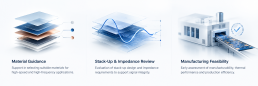
PCB performance is influenced by more than material selection alone. Stack-up design, impedance requirements, thermal behavior and manufacturing feasibility all need to be considered early in the development process.
PCB Connect works closely with customers and manufacturing partners to evaluate dielectric properties, signal loss, controlled impedance, layer stack-up, thermal performance and overall manufacturing feasibility. Cost efficiency is also considered to help balance technical performance with production requirements.
This supports better material and technology decisions before production, helping reduce technical risk and create a more efficient development process.
Manufacturing Quality & Verification
Advanced manufacturing and quality control processes help ensure consistent PCB performance in demanding telecom applications.
Laser Direct Imaging (LDI)
Supports high pattern accuracy for fine features and complex PCB designs.
Automated Optical Inspection (AOI)
Detects surface defects and pattern deviations during production.
X-ray Inspection & Impedance Verification
Enables inspection of internal structures while supporting verification of controlled impedance requirements.
Electrical Testing
Confirms electrical continuity and helps identify faults before delivery.
Process Monitoring & Traceability
Supports production control, documentation and traceability throughout the manufacturing process.
Quality Management Systems
Structured quality processes help maintain consistency, manage deviations and support long-term production reliability.
FAQ
Common Customer Questions
Low-loss and ultra-low-loss laminates are typically recommended when signal integrity and insertion loss become critical design factors.
Yes.
We support PCB solutions for RF, microwave, and millimeter-wave applications, including controlled impedance and advanced material requirements.
Yes.
We support projects from early-stage prototypes through full-scale production and long-term supply programs.
We support 5G infrastructure, networking equipment, optical communications, satellite systems, antenna technologies, RF equipment, and connected IoT devices.
Our manufacturing partners utilize advanced inspection and testing technologies, including AOI, X-ray inspection, electrical testing, and controlled process management.
Your Telecom PCB Partner
Contact PCB Connect to discuss your technical requirements and identify the optimal PCB solution for your application.